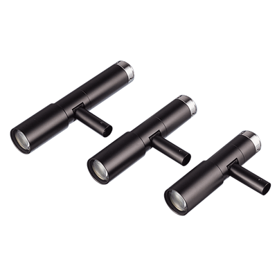
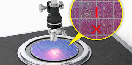
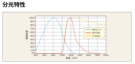
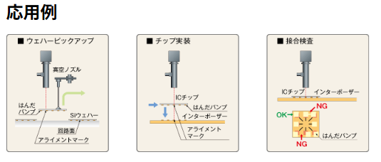
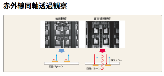
▪ Dedicated infrared design (850~1700 nm) ▪ By combined it with an infrared-compatible cameras and lighting, it supports special applications that can observe defects inside wafers and patterns on the back side. ▪ High magnification models ▪ Uniform coaxial illumination functionality covering the entire field of view