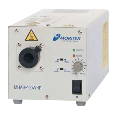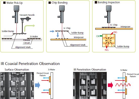
• Observation of images that are not visible • Void inspections • SAW filter (LiNbO3 LiTaO3) inspections • MEMS inspections • Wafer on wafer positioning • FCB positioning • Image recognition through film • Wiring recognition on TAB circuit boards • Wafer surface observation/ OCR • Infrared microscope lighting
* Lamps other than compatible lamps cannot be used.

MORITEX North America, Inc.
Add:20380 Town Center Lane, Suite 215 Cupertino, CA 95014 USA.
Tel:+1-408-363-2100
Site Policy | Privacy-Policy | Help | @ 2023 MORITEX Corporation